- 您现在的位置:买卖IC网 > Sheet目录479 > MRF89XA-I/MQ (Microchip Technology)TXRX ISM SUB-GHZ ULP 32QFN
�� �
�
�MRF89XA�
�2.2� Reset� Pin�
�The� device� enters� the� Reset� mode� if� any� of� the�
�following� events� take� place:�
�The� PA� and� the� LNA� front-ends� in� the� MRF89XA,� which�
�share� the� same� Input/Output� pin,� are� internally�
�matched� to� approximately� 50� Ω� .�
�?� Power-on� Reset� (POR)�
�2.4�
�Filters� and� Amplifiers� Block�
�?� Manual� Reset�
�The� POR� happens� when� the� MRF89XA� is� switched� on�
�using� V� DD� .� The� POR� cycle� takes� at� least� 10� ms� to�
�execute� any� communication� operations� on� the� SPI� bus.�
�An� external� hardware� or� manual� Reset� of� the�
�MRF89XA� can� be� performed� by� asserting� the� TEST8�
�pin� (pin� 13)� to� high� for� 100� μs� and� then� releasing� the�
�pin.� After� releasing� the� pin,� it� takes� more� than� 5� ms� for�
�the� transceiver� to� be� ready� for� any� operations.� The� pin�
�is� driven� with� an� open-drain� output,� therefore,� is� pulled�
�high� while� the� device� is� in� POR.� The� device� will� not�
�accept� commands� during� the� Reset� period.� For� more�
�information,� refer� to� Section� 3.1.2,� Manual� Reset� .�
�2.4.1� INTERPOLATION� FILTER�
�After� digital-to-analog� conversion� during� transmission,�
�both� I� and� Q� signals� are� smoothed� by� interpolation�
�filters.� These� low-pass� filters� the� digitally� generated�
�signal,� and� prevents� the� alias� signals� from� entering� the�
�modulators.�
�2.4.2� POWER� AMPLIFIER�
�The� Power� Amplifier� (PA)� integrated� in� the� MRF89XA�
�operates� under� a� regulated� voltage� supply� of� 1.8V.� The�
�external� RF� choke� inductor� is� biased� by� an� internal�
�regulator� output� made� available� on� the� PARS� pin� (pin�
�29).� Therefore,� the� PA� output� power� is� consistent� over�
�2.3�
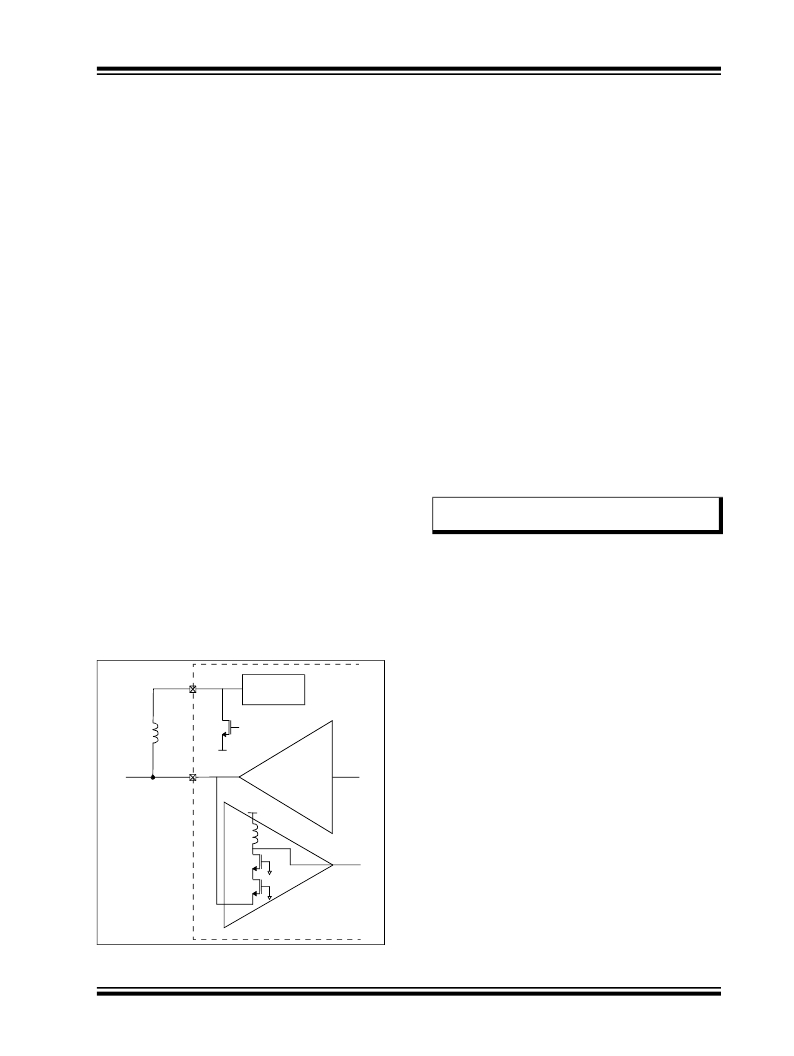
�RFIO� Pin�
�the� power� supply� range.� This� is� important� for�
�applications� which� allows� both� predictable� RF�
�The� receiver� and� the� transmitter� share� the� same� RFIO�
�pin� (pin� 31).� Figure� 2-3� illustrates� the� configuration� of�
�the� common� RF� front-end.�
�?� In� Transmit� mode,� the� PA� and� the� PA� regulator�
�are� ON� with� voltage� on� the� PARS� pin� (pin� 29)�
�performance� and� battery� life.�
�An� open� collector� output� requires� biasing� using� an�
�inductor� as� an� RF� choke.� For� the� recommended� PA�
�bias� and� matching� circuit� details� see� Section� 4.4.2,�
�Suggested� PA� Biasing� And� Matching� .�
�equal� to� the� nominal� voltage� of� the� regulator�
�(about� 1.8V).� The� external� RF� choke� inductance�
�is� used� to� bias� the� PA.�
�Note:�
�Image� rejection� is� achieved� using� a� SAW�
�filter� on� the� RF� input.�
�?� In� Receive� mode,� the� PA� and� PA� regulator� are�
�OFF� and� PARS� is� tied� to� ground.� The� external� RF�
�choke� inductor� is� used� for� biasing� and� matching�
�the� LNA� (this� is� basically� implemented� as� a� com-�
�mon� gate� amplifier).�
�The� matching� of� the� SAW� filter� depends� on� the� SAW�
�filter� selected.� Many� modern� SAW� filters� have� 50� Ω�
�input� and� output,� which� simplifies� matching� for� the�
�MRF89XA.� This� is� demonstrated� in� the� application�
�circuit.� If� the� choice� of� SAW� filter� is� different� than� 50� Ω� ,�
�the� required� impedance� match� on� the� input� and� output�
�FIGURE� 2-3:�
�COMMON� RF� INPUT� AND�
�of� the� SAW� filter� will� be� needed.�
�OUTPUT� PIN� DIAGRAM�
�2.4.3�
�LOW� NOISE� AMPLIFIER�
�(WITH�
�PARS�
�PA� Regulator�
�(1.8V)�
�RX� ON�
�FIRST� MIXER)�
�In� Receive� mode,� the� RFIO� pin� (pin� 31)� is� connected� to�
�a� fixed� gain,� common-gate,� Low� Noise� Amplifier� (LNA).�
�The� performance� of� this� amplifier� is� such� that� the� Noise�
�Figure� (NF)� of� the� receiver� is� estimated� to� be�
�approximately� 7� dB.�
�To�
�Antenna�
�RFIO�
�PA�
�The� LNA� has� approximately� 50� Ω� impedance,� which�
�functions� well� with� the� proposed� antenna� (PCB/�
�Monopole)� during� signal� transmission.� The� LNA� is� fol-�
�lowed� by� an� internal� RF� band-pass� filter.�
�LNA�
�?� 2010–2011� Microchip� Technology� Inc.�
�Preliminary�
�DS70622C-page� 15�
�发布紧急采购,3分钟左右您将得到回复。
相关PDF资料
MRF89XAM9A-I/RM
IC TXRX MOD 915MHZ ULP SUB-GHZ
MRX-001-433DR-B
MODULE RECEIVER 433MHZ 18DIP
MRX-002-433DR-B
MODULE RECEIVER 433MHZ 18DIP
MRX-002SL-433DR-B
MODULE RCVR 433MHZ SAW LN 24DIP
MRX-005-915DR-B
MODULE RECEIVER 915MHZ 18DIP
MRX-005SL-915DR-B
MODULE RCVR 915MHZ SAW LN 24DIP
MRX-007-433DR-B
MODULE RECEIVER 433MHZ 18DIP
MRX-008-433DR-B
MODULE RECEIVER 433MHZ 18DIP
相关代理商/技术参数
MRF89XAM8A-I
制造商:MICROCHIP 制造商全称:Microchip Technology 功能描述:Ultra Low-Power, Integrated ISM Band Sub-GHz Transceiver
MRF89XAM8A-I/RM
功能描述:射频模块 868MHz Sub-GHz transceiver module
RoHS:否 制造商:Linx Technologies 产品:Transceiver Modules 频带:902 MHz to 928 MHz 输出功率:- 15.5 dBm to + 12.5 dBm 接口类型:UART 工作电源电压:- 0.3 VDC to + 5.5 VDC 传输供电电流:38.1 mA 接收供电电流:22.7 mA 天线连接器类型:U.FL 最大工作温度:+ 85 C 尺寸:1.15 mm x 0.63 mm x 0.131 mm
MRF89XAM8A-I/RM
制造商:Microchip Technology Inc 功能描述:, Leaded Process Compatible:Yes, Peak Re
MRF89XAM9A_12
制造商:MICROCHIP 制造商全称:Microchip Technology 功能描述:915 MHz Ultra Low-Power Sub-GHz Transceiver Module
MRF89XAM9A-I/RM
功能描述:射频模块 915MHz Sub-GHz Transceiver Mod RoHS:否 制造商:Linx Technologies 产品:Transceiver Modules 频带:902 MHz to 928 MHz 输出功率:- 15.5 dBm to + 12.5 dBm 接口类型:UART 工作电源电压:- 0.3 VDC to + 5.5 VDC 传输供电电流:38.1 mA 接收供电电流:22.7 mA 天线连接器类型:U.FL 最大工作温度:+ 85 C 尺寸:1.15 mm x 0.63 mm x 0.131 mm
MRF89XAM9AT-I/RM
制造商:Microchip Technology Inc 功能描述:915 MHz Ultra Low-Power Sub-GHz Transceiver Module
MRF89XAT-I/MQ
功能描述:射频收发器 868/915/950 MHz Sub-GHz transceiver RoHS:否 制造商:Atmel 频率范围:2322 MHz to 2527 MHz 最大数据速率:2000 Kbps 调制格式:OQPSK 输出功率:4 dBm 类型: 工作电源电压:1.8 V to 3.6 V 最大工作温度:+ 85 C 接口类型:SPI 封装 / 箱体:QFN-32 封装:Tray
MRF8HP21080HR3
功能描述:射频MOSFET电源晶体管 HV8 2.1GHZ 160W NI780H-4 RoHS:否 制造商:Freescale Semiconductor 配置:Single 晶体管极性: 频率:1800 MHz to 2000 MHz 增益:27 dB 输出功率:100 W 汲极/源极击穿电压: 漏极连续电流: 闸/源击穿电压: 最大工作温度: 封装 / 箱体:NI-780-4 封装:Tray